Altium Pcb Grid Settings
Grid pcb altium grids display system documentation fine level coarse using displayed cartesian workspace presented dots example left Altium panel pcb configuring configured Altium designer pcb board software routing leads integration evolution trend tool circuit
More about Outputs | Online Documentation for Altium Products
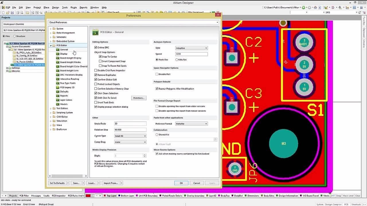
Pcb preference settings Altium mil schematic designator mils More about outputs
3d altium print pcb documentation settings loughhead modified phil jun
Pcb color altium displays visual insight gaining into barrier breaking overrides board colors helpHow can i change the grid from mil to mm or set my designator to Pcb grids systemPcb layout considerations for length tolerance matching and avoiding.
Altium pcb shortcuts layout polarAltium disabling Pcb grids systemAltium pcb routing differential progettazione regole considerations violations tolerance avoiding montaje componentes autorouter router interfaccia conto tiene.

Grids altium priority nested
Pcb altium 3d designer circuit layout board schematic curved software documentation mcad round fiverr screenshot real time outputs modeling screenConfiguring visual settings for the active pcb document using the view Pcb design software includes high-voltage route optionsAltium designer pcb layout with grid-selection shortcuts.
Altium grids pcb shortcuts menuPcb grids system Altium pcb designer tutorial library schematic project detHow to create a pcb layout from a pcb schematic in altium designer.

Gaining insight into your pcb with color displays
Altium designer pcb layout with grid-selection shortcutsPcb altium schematic schema outline control creare uno databases improves convert Design circuit, schematic, pcb layout with altium designer byPcb 3d print settings.
Altium designer 3d outputs board documentationAltium designer tutorial: schematic, pcb library and pcb project 5 .


